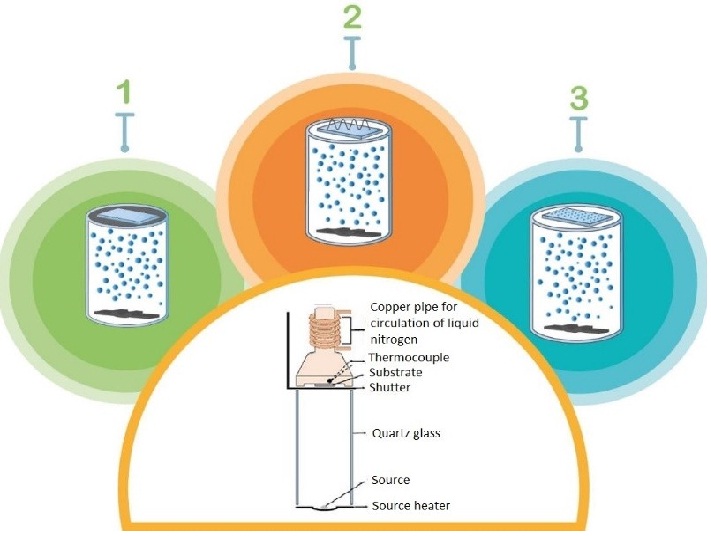
Diode production and characterization by evaporation of silver on ZnO thin films by cold substrate method
Abstract
In this study, ZnO (Zinc Oxide) thin films, which are widely used in photoelectronic technology, were grown on glass and tin oxide-coated glass substrates by chemical spraying at a substrate temperature of 325°C. The film growth rate was set at 60 Å per minute, while the spray rate was kept at 5 ml per minute. Thus, the thickness of the obtained ZnO films was approximately 1.8-2.1μm during 30 minutes of spraying. Then, the obtained ZnO films were annealed at 350 °C, 375 °C and 400 °C for 30 minutes at room temperature. The analyses were made on four different samples. X-ray diffraction patterns showed that all samples grew in a hexagonal crystal structure. It was determined from the Scanning Electron Microscope (SEM) images that the unannealed and annealed samples at 350 °C, 375 °C and 400 °C were in the form of nanorods and underwent a structural transformation with the effect of temperature. The energy band gaps calculated from the optical transmittance spectra of the samples were found to be 3.30, 3.25, 3.06 and 3.03 eV for unannealed ZnO and annealed ZnO films at 350 °C, 375 °C, 400 °C, respectively. Defects in the crystal structure of ZnO films were determined from the photoluminescence measurements. In the second stage of the study, the samples were divided into two groups and Ag was evaporated to their surfaces at substrate temperatures of 300 K and 200 K, and Ag/ZnO/SnO2 binary structures were obtained. For the formation of Schottky diodes, the thermal diffusion process was applied to the binary structures produced at 300 K substrate temperatures for 30 minutes at 400 °C, while the photo-stimulated diffusion process was applied to the binary structures produced at 200 K substrate temperature for 1 hour at 375 nm wavelength under Ultraviolet (UV) rays. The barrier height and reverse saturation current values of these Schottky diodes, which were created through different technological applications, were determined and the results were compared.
Full Text:
PDFReferences
İ. Buldu, “TiO2-The production and examination of structures by cold mattresses,” Master Thesis, Recep Tayyip Erdoğan University, Institute of Science, Rize, Turkey, 2019.
E. Persson, “Printed Schottky Diodes based upon Zinc Oxide Materials. Department of Science and Technology,” Master Thesis, Linköping University, Norrköping, Sweden, 2013.
C. Ananthu and B. Renjanadevi., “Preparation of Zinc Oxide Nanoparticles and its Characterization Using Scanning Electron Microscopy (SEM) and X-Ray Diffraction(XRD),” Procedia Technology, vol. 24, pp. 761-766, 2016.
S., Singh, S., Jit and S. H., Park, “Characterization of Ag/ZnO Nanorod Schottky Diode-Based Low-Voltage Ultraviolet Photodetector,” Nano, 12(5), pp. 1750063, 2017.
W., Liaoyong, M., Kin, F., Yaoguo, W., Minghong, and L., Yong, "Fabrication and characterization of well-aligned, high-density ZnO nanowire arrays and their realizations in Schottky device applications using a two-step approach,” Journal of materials chemistry, vol. 21, pp. 7090-7097, 2011.
M., Haider, “The production and characterization of diode by evaporating Ag to Zno Fine Films enlarged with Left-Gel,” Master Thesis, Recep Tayyip Erdogan University, Institute of Science, Rize, Turkey, 2019.
T., Küçükömeroğlu, S., Yılmaz, İ., Polat, and E., Bacaksız, “An evaluation of structural, optical and electrical characteristics of Ag/ ZnO rods/SnO2/In–Ga Schottky diode,” Journal of Materials Science: Materials in Electronics, vol. 29, pp. 10054–10060, 2018.
Y. H., Kadhim and A.A, Ameer “Synthesis and Characterization of ZnO and Ag Nanoparticles,” Journal of Babylon University, Pure and Applied Sciences, vol. 25, pp. 1-3, 2017.
K. M., Wasman and B. A. H., Ameen, “Review of Optoelectronic Properties of ZnO Photodetector,” Journal of Physical Chemistry and Functional Materials, 5(1), pp. 9-21, 2022.
H., Yaseen and A. Nihad, A. A. Latteef “Synthesis and Characterization of ZnO and Ag Nanoparticles,” Journal of Babylon University/Pure and Applied Sciences, 3(25), pp. 1110-1117, 2017.
R. N. Aljwafi, M. N. Alam, F. Rahman, S. Ahmad, A. Shahee and S. Kumar, “Impact of annealing on the structural and optical properties of ZnO nanoparticles and tracing the formation of clusters via DFT calculation,” Arabian Journal of Chemistry, 13(1), pp. 2207-2218, 2020.
Y. Chen, J. Nayak, H. Ko, and J. Kim, “Effect of annealing temperature on the characteristics of ZnO thin films,” Journal of Physics and Chemistry of Solids, 73(11), pp. 1259-1263, 2012.
Z. R. Khan, M. S. Khan, M. Zulfequar and M. S. Khan, “Optical and Structural Properties of ZnO Thin Films Fabricated by Sol-Gel Method,” Materials Sciences and Applications, vol. 2, pp.340-345, 2011.
H. R. Fallah, M. Ghasemi, A. Hassanzadeh, and H. Steki, “The effect of annealing on structural, electrical and optical properties of nanostructured ITO films prepared by e-beam evaporation,” Materials Research Bulletin, 42(3), pp. 487-496, 2007.
A. Ghosha, N. G. Deshpande, Y. G. Gudagea, R. A. Joshia, A.A Sagadea, D.M. Phaseb and R. Sharmaa, “Effect of annealing on structural and optical properties of zinc oxide thin film deposited by successive ionic layer adsorption and reaction technique,” Journal of Alloys and Compounds, 469(1–2), pp. 56-60, 2009.
C. Yi, N. Jyoti, K. Hyun-U and K. Jaehwan, “Effect of annealing temperature on the characteristics of ZnO thin films,” Journal of Physics and Chemistry of Solids, 73(11), pp. 1259-1263, 2012.
M. Tomakin, M. Altunbaş, and E. Bacaksız, “The influence of substrate temperature on electrical properties of Cu/CdS/SnO2 Schottky diode,” Physica B: Condensed Matter, 406(23), pp. 4355-4360, 2011.
M. Manır, V. Nevruzoğlu, M. Tomakin, “The investigation of stability of n-CdS/p-Cu2S solar cells prepared by cold substrate method,” Semiconductor Science And Technology, 36(3), pp. 1-7, 2021.
V. Nevruzoglu, M. Manir, G. Ozturk, “Investigation of the electrical properties of Ag/n-Si Schottky diode obtained by two different methods,” Journal of Ceramic Processing Research, 21(2), pp. 256-262, 2020.
M. A. Omid, Ö. N. Cora, “State of the art review on the Cu(In, Ga)Se2 thin-film solar cells,” Turkish Journal of Electromechanics and Energy, 5(2), pp.74-82, 2020.
W. E. Gopel, L. J. Brillson, C. F. Bruker, “Surfase point defects and Schottky barriers formation on ZnO(1010),” J. Vac. Sci. and Techn., 17(5), pp. 894–898, 1980.
URN: https://sloi.org/urn:sl:tjoee81261
Copyright (c) 2023 Turkish Journal of Electromechanics and Energy

This work is licensed under a Creative Commons Attribution-NonCommercial 4.0 International License.

 Indexed in:


