Atomic Layer Deposition (ALD) of Vanadium Oxide Thin Films
Abstract
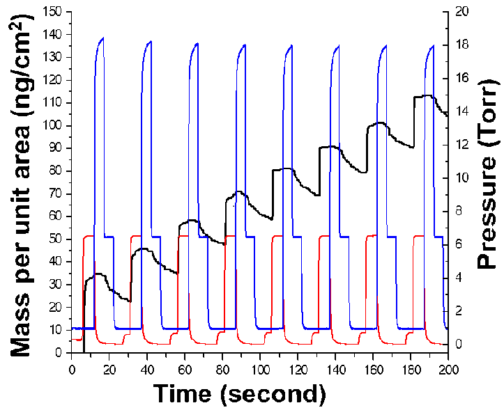
Microbolometer grade vanadium oxide thin films were grown by Atomic Layer Deposition (ALD) method using VTIP metal organic precursor and water vapor. The ALD process was studied using in-situ QCM system integrated into the reactor. Mass uptake during each half reaction was monitored and analyzed for different half-reaction sequences. An overall mass uptake of 20 ng/cm2 was recorded for a complete ALD cycle. Thickness analysis of the vanadium oxide films grown by 2500 cycles yielded a thickness of ~800 Å which corresponds to a 0.32 Å /cycle thin film growth rate. The ALD grown thin films were characterized and their electrical and structural properties were reported. Temperature coefficient of resistance (TCR) value was measured to be around -4.7%/K, and resistivity was found as 77kΩ.cm. In addition, the ALD grown vanadium oxide thin films are found to be oxygen reach in composition that is yielding V2O5.
References
R. R. Kumar, Pulsed laser deposited vanadium oxide thin films for uncooled infrared detectors, Sensors Actuators A Phys., 107(1), 62–67 (2003).
B. D. Gauntt, Microstructure of Vanadium Oxide Used in Microbolometers, in Proceedings of SPIE, 8012(1), 80123T-80123T–7, (2017).
A. Ozcelik, O. Cabarcos, D. L. Allara, and M. W. Horn, Vanadium Oxide Thin Films Alloyed with Ti, Zr, Nb, and Mo for Uncooled Infrared Imaging Applications, J. Electron. Mater., 42(5), 901-905 (2013).
Y. Lv, M. Hu, M. Wu, and Z. Liu, Preparation of vanadium oxide thin films with high temperature coefficient of resistance by facing targets d.c. reactive sputtering and annealing process, Surf. Coatings Technol., 201(9–11), 4969–4972, (2007).
S. Chen et al., Vanadium oxide thin films deposited on silicon dioxide buffer layers by magnetron sputtering, Thin Solid Films, 497(1–2), 267–269, (2006).
E. E. Chain, Optical properties of vanadium dioxide and vanadium pentoxide thin films., Appl. Opt., 30(19), 2782–7, (1991).
Y.-H. Han, K. Kim, N. Chi-anh, and H. Shin, Fabrication and characterization of bolometric oxide thin film based on vanadium–tungsten alloy, Sensors Actuators A Phys., (123), 660–664, (2005).
Y. Jin, A. B. Hitesh, A. Ozcelik, N. J. Tom, and W. H. Mark, High resistivity and high TCR vanadium oxide thin films for infrared imaging prepared by bias target ion beam deposition, in Proceedings of SPIE - The International Society for Optical Engineering, 8704, (2013).
A. Rogalski, Infrared Detectors (Electrocomponent Science Monographs, Volume 10). CRC Press, (2000).
P. W. Kruse, Uncooled Thermal Imaging: Arrays, Systems, and Applications. Bellingham: SPIE Press, (2001).
S. Baranovski, Charge transport in disordered solids with applications in electronics. John Wiley and Sons, (2006).
S. S. N. Bharadwaja, C. Venkatasubramanian, N. Fieldhouse, S. Ashok, M. W. Horn, and T. N. Jackson, Low temperature charge carrier hopping transport mechanism in vanadium oxide thin films grown using pulsed dc sputtering, Appl. Phys. Lett., 94(22), 222110, (2009).
C. Venkatasubramanian, M. W. Horn, and S. Ashok, Ion implantation studies on VOx films prepared by pulsed dc reactive sputtering, Nucl. Instruments Methods Phys. Res. Sect. B Beam Interact. with Mater. Atoms, 267(8–9), 1476–1479, (2009).
J. Li, B. D. Gauntt, and E. C. Dickey, Microtwinning in highly nonstoichiometric VOx thin films, Acta Mater., 58(15), 5009–5014, (2010).
N. Fieldhouse, S. M. Pursel, M. W. Horn, and S. S. N. Bharadwaja, Electrical properties of vanadium oxide thin films for bolometer applications: processed by pulse dc sputtering, J. Phys. D. Appl. Phys., 42(5), 055408, (2009).
C. Venkatasubramanian, O. M. Cabarcos, D. L. Allara, M. W. Horn, and S. Ashok, Correlation of temperature response and structure of annealed VOx thin films for IR detector applications, J. Vac. Sci. Technol. A Vacuum, Surfaces, Film., 27(4), 956, (2009).
R. L. Puurunen, Surface chemistry of atomic layer deposition: A case study for the trimethylaluminum/water process, J. Appl. Phys., vol. 97(12), 121301, (2005).
J. W. Elam, M. D. Groner, and S. M. George, Viscous flow reactor with quartz crystal microbalance for thin film growth by atomic layer deposition, Rev. Sci. Instrum., 73(8), 2981, (2002).
R. A. Wind and S. M. George, Quartz crystal microbalance studies of Al2O3 atomic layer deposition using trimethylaluminum and water at 125 degrees C., J. Phys. Chem. A, 114(3), 1281–9, (2010).
C. F. Herrmann, Properties of atomic layer deposited Al2O3/ZnO dielectric films grown at low temperature for RF MEMS, SPIE, 5715 (2005).
I. M. Povey, M. Bardosova, F. Chalvet, M. E. Pemble, and H. M. Yates, Atomic layer deposition for the fabrication of 3D photonic crystals structures: Growth of Al2O3 and VO2 photonic crystal systems, Surf. Coatings Technol., 201(22–23), 9345–9348, (2007).
J. Musschoot et al., Comparison of Thermal and Plasma-Enhanced ALD/CVD of Vanadium Pentoxide, J. Electrochem. Soc., 156(7), P122, (2009).
P. Dagur, A. Mane, and S. Shivasankar, Thin films of VO on glass by atomic layer deposition: microstructure and electrical properties, J. Cryst. Growth, 275(1–2), e1223–e1228, (2005).
J. C. Badot, a. Mantoux, N. Baffier, O. Dubrunfaut, and D. Lincot, Electrical properties of V2O5 thin films obtained by atomic layer deposition (ALD), J. Mater. Chem., 14( 23), 3411, (2004).
T. J. Larrabee, T. E. Mallouk, and D. L. Allara, An atomic layer deposition reactor with dose quantification for precursor adsorption and reactivity studies, Rev. Sci. Instrum., 84(1), 014102, (2013).
G. Sauerbrey, Verwendung von Schwingquarzen zur Wägung dünner Schichten und zur Mikrowägung, Zeitschrift für Phys., 155(2), 206–222, (1959).
URN: https://sloi.org/urn:sl:tjoee42146
Copyright (c) 2019 Turkish Journal of Electromechanics and Energy

This work is licensed under a Creative Commons Attribution-NonCommercial 4.0 International License.

 Indexed in:


![]()


![]()

![]()


![]()
![]()
![]()

![]()